6.1. Model Validation Using Impedance Response
For the purpose of validating the model created of the motorette testbed, the impedance responses of the model and testbed were compared. The testbed impedance response was found by supplying the coil under test with a range of square wave impulses between 5 ms and 500 µs by changing the output frequency and duty cycle from the power module and is shown in
Figure 16. Due to hardware limitations of the system level controller, pulses exceeding 5 ms and shorter than 500 µs were not tested. This process was conducted with pulse amplitudes of 480 V, 1 kV, and 4 kV, but no change was found in the impedance response. A handheld BK Precision 880 LCR meter was also used to measure the impedance at select frequencies.
As can be seen in
Figure 16, there is close alignment between the impedance response of the model and the testbed results. The differences at lower frequencies are likely due to the upper limit on the pulse durations of 5 ms for the ETFE analysis as this limits the resolution of the lower frequency response data. Additionally, as the model only implements the 1 MHz mutual inductance and resistance it is expected that the model would have a more accurate representation at frequencies around 1 MHz. However, at frequencies above 5 MHz the model predictions become unstable due to simplifications in the modeling process, such as the simplification of skin effects and limits to the ladder circuit order. Additionally, for frequencies above 5 MHz, the noise level of the testbed produces distortion and uncertainty. Also of note is the diminished peak impedance of the testbed results of the XHV-9 in comparison to the XHV-6 and DEI results; this is due to the changes in the circuit topology discussed earlier that were done to increase stability of the power circuit.
After the general modeling process for a healthy coil was validated, the method for modeling the impact of air-filled voids and insulation delamination was validated using the milled coil discussed earlier. The changes to the impedance of the MCTL model with and without delamination are compared to the testbed results of the coil before and after the turn 1 insulation was milled down in
Figure 17. As the XHV-9 testbed was used for testing, the peak impedance is diminished; thus, a direct comparison of the undamaged and 0.5 mm milled impedances cannot be made. Nonetheless it can still be observed that both the MCTL model and the testbed results experienced equivalent peak shifts with the resonant frequency changing from approximately 2.97 MHz to 3.06 MHz with a gain increase of about 0.6 dB. As can be understood from the analytical impedance model of a ladder circuit, both the MCTL model and the testbed experienced a reduction of the GW capacitance of the same amount; this is in line with expectations based on dielectric theory, thus validating the modeling approach for insulation abnormalities.
6.2. Simulation of the Overvoltage Phenominom and Voltage Distribution of the Coils
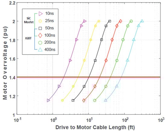
With the impedance response of the MCTL model validated through comparison to testbed results it is possible to use the proposed single coil model to simulate the response of a full phase of a stator winding. To do so, a simulation model was created that consists of eight coils placed in series. The coils are connected to a pulse generator with a 2 m lossy transmission line whose p.u. impedance was modeled to reflect the cable used on the testbed. Additionally, it is assumed that the neutral point of the machine is grounded, thus the output of the last coil model is also grounded. The impulse response of the simulation model when excited with a 100 kHz impulse with an amplitude of 2400 V and a rise time of 20 ns is shown in
Figure 18. It can be clearly seen that the voltage of the first coil experiences the highest overshoot and a higher frequency oscillation than the other coils; this is expected for a setup with a grounded nutral point. Because this simulation is designed to reflect a more real world application instead of a worst case scenario (i.e., long cables with a high impedance mismatch), the voltage overshoot at coil 1 is only 22.88%. However, when the simulation was repeated with a 100 ns rise time to represent operation by a Si inverter, the overshoot was limited to 7.5%, meaning the SiC operation represented a three times increase in the percent overvoltage.
As discussed above, another key area of concern for modeling the electrical stress placed in stator insulation is the voltage difference between adjacent conductors. The voltage differences between turns 1 and 2, 3 and 4, and 5 and 6 for the first coil using the same simulation setup as described above are shown in
Figure 19. Due to the fixed nature of the turn positions within a form wound coil, the potential issue of the first and last turns becoming adjacent is never an issue; nonetheless, the TT insulation can still experience high voltage potentials especially near the machine terminals.
Figure 19 illustrates that for a brief period of every cycle, the TT insulation between turns 1 and 2 experiences the full electric potential of the DC bus voltage. To further investigate this, the proposed method of using the turn voltages from the MCTL model as an impetus for the FEM model can be employed as is discussed below.
6.3. Modeling the Impact of Delaminations on Electrical Stress
After the modeling process is validated both for a healthy system and a system with air-filled voids within the insulation, the modeling process can be expanded to investigate additional testcases and the resulting electrical stress on the insulation in greater detail by importing the conductor voltages into the COMSOL model as described earlier. For this work, the primary area of interest of the COMSOL voltage distribution model is the areas of the insulation experiencing electric field densities exceeding 3 kV/mm. This threshold for electrical stress was selected because prior studies have found that insulation experiences accelerated aging and partial discharge behavior at this level, thus an electric field density of 3 kV/mm or more is considered high stress [
50]. For these tests the baseline is a coil without damage to the insulation that experiences a 20 kHz excitation wave with a rise time of 20 ns. These results were also compared to the electric stress estimations if it is assumed that the coil is energized with an ideal voltage square wave with no overvoltage; this was done to illustrate the importance of modeling the actual coil voltages. The simulations conducted that do not consider the overvoltage phenomenon are marked as Square Impulse. Additionally, simulations were run with rise times of 100 ns to represent the electric stress on the insulation that would be created if the coil was operated by a Si inverter. The tests discussed are focused on impulses with a DC bus ranging from 2400 V to 4160 V as it was found that coils with voltages in this region experienced the most transient behavior.
The first simulation was to investigate the impact of the location of a delamination on the insulation stress. A delamination was modeled adjacent to the turn 1 conductor, at the midpoint between the conductor and the GW, and adjacent to the GW; the results of this simulation are shown in
Figure 20. The figure shows the mean percent of the insulation that exceeded the 3 kV/mm threshold over the course of a full impulse, the maximum instantaneous area of the insulation above the damage threshold, and the maximum electric field present in the insulation over the impulse cycle. As can be seen across all stress factors considered, the modeling approach proposed by this work predicts higher insulation stress than a model which neglects the transmission line behavior of the coil. This disparity is increasingly prevalent as the excitation voltage of the system increases.
The presence of a delamination in the insulation increases the maximum electric field experienced by the insulation with the maximum field increasing proportionally to the proximity of the delamination to the conductor. This relationship was also consistent for the mean percent of the insulation area exceeding 3 kV/mm. The presence of a delamination increased the mean area under high stress with this area further increased as the delamination is moved closer to the conductor. However, these changes were not as impactful as those to the maximum electric field that had an increase in the electric field maximum of about 23%, while the percent difference of the mean stressed area between the healthy model and a delaminated model was ~5%.
This is expected as the maximum electric field within the insulation is heavily dependent on the overvoltage oscillations and local electric fields within only a small part of the insulation, the immediate area surrounding the maxima; thus, even a small change to the insulation can have a profound impact. By contrast the maximum and mean areas of the insulation experiencing high stress both consider the entire insulation area, making them more desensitized to small changes, such as a void or delamination.
The trend of an increase in severity of the stress metric for delamination closer to the conductor that was observed, with both the maximum electric field and mean area of insulation exceeding 3 kV/mm, was also true for the maximum instantaneous percent of the insulation that exceeded the damage threshold for voltages less than 3500 V. However, as the excitation voltage increases from 3500 V to voltages up to 4000 V the behavior shifts such that proximity of a delamination to the conductor slightly reduces the maximum percent of the insulation area to experience fields above 3 kV/mm. This phenomenon was further investigated with
Figure 21 illustrating why this behavior is occurring.
The figures show the electric field of the region around the left conductor of turn 1 when the model is excited with 3 kV, 3.5 kV, and 4 kV pulses when the insulation is both healthy and when there are delaminations present. The instant of the maximum electric field in this region is shown. Only those parts of the insulation experiencing electric fields of 3 kV/mm or more are shown for the sake of clearly illustrating the behavior.
The presence of the delamination concentrates the electric field density in the air-filled region. At lower voltages this region would not normally exceed 3 kV/mm (a); thus, the concentration created by the delamination increases that area to above the 3 kV/mm threshold when it would not normally. At voltages above 4 kV, the electric field saturation of the insulation is sufficiently high that even the reduction created by the field concentration inside the airgap does not lower the overall field bellow the 3 kV/mm threshold as seen in
Figure 21c,f,i. However, for voltages between 3500 V and 4000 V, there is an area of the insulation that would normally exceed 3 kV/mm, but due to the field concentration is lowered to below the threshold. As this phenomenon is dependent on the electric field distribution within the insulation, position and size of the damage and voltage level of the surrounding conductors, the voltage level of occurrence and impact is expected to change for each application. This behavior should not be taken out of context by insinuating that a delamination can reduce the stress on the insulation as this is only a marginal change to one of the stress metrics tracked by this study; both of the other stress metrics show a sizable increase in severity with the presence of a delamination, most notably the maximum electric field within the insulation which has been studied at length in regards to its role in partial discharge activity.
Following this, simulations examining the impact of rise time on the insulation stress were performed. The model was simulated with a rise time of 20 ns to represent a SiC device and 100 ns to represent a Si device. Both were simulated with healthy insulation and with delamination and voids. A selection of results is shown in
Figure 22. As is expected, based on overvoltage theory, tests with a 20 ns rise time experience noticeably increased stress across all test points when compared to equivalent tests with a 100 ns rise time. This clearly illustrates the increased stress placed on insulation by SiC operation when compared to Si operation for all test cases, thus necessitating the adaptation of stress prediction methods to account for a change from Si to SiC.
The impact of voids was also investigated and compared to the impact of delamination on the insulation. As detailed above, small circular air-filled voids were added to the southwest corner of the insulation near turns 1 and 7; the delamination condition considered for this test is a midpoint delamination. The results of these tests are shown in
Figure 23. The presence of voids resulted in a slight increase in all three-stress metrics in comparison to the baseline non-damaged insulation model, but they did not have the same magnitude of impact as a delamination. This is expected because the overall area of insulation altered by a delamination is significantly larger than that of a void. The reduced area of voids also means that the phenomenon where the maximum area to exceed 3 kV/mm is decreased in the presence of a delamination for voltages between 3500 V and 4000 V is not as prevalent.
6.4. Results of SoH Tracking with Aged Coils
To showcase the ability to trend data collected during online operation of a motor coil additional accelerated aging tests were performed. Following the method presented by Tsykhla [
41], a single capacitance value was extracted from each of the frequency dependent capacitances found at each time instance. The changes in the capacitance of the 2400 V coil tested at 4 kV and 60 °C are shown in
Figure 24 where 20 samples were collected at each aging time. As can be seen, there is a clear decrease in the insulation equivalent capacitance as the coil undergoes accelerated aging.
The other method investigated for tracking the SoH of the coil insulation was the examination of changes to the coil inrush current oscillations. A similar process to that used for the GW equivalent circuit tracking was employed whereby the current oscillations of several impulses were collected for each of the SoH test conditions for both the coil inrush current and the coil GW leakage current. The current spectrum amplitudes for a selection of the test conditions using the input current are shown in
Figure 25. As this metric is focused on the high frequency behavior of the coil current, the readings are more susceptible to noise. Nonetheless, it is evident that there are shifts in the maxima of the current spectrum as the coil is aged, most specifically the 1st, 2nd, and 3rd maxima.
In 10 h intervals during the accelerated aging test, 20 samples of the HF current spectrum were collected for both the input current and the GW leakage current. The ISI, as discussed by Nussbaumer [
42], of the coil was calculated for the coil current and leakage current and is shown in
Figure 26 for coils aged at 60 °C,
Figure 26a and
Figure 26b, and 120 °C,
Figure 26c and
Figure 26d, respectively [
47].
The results of the ISI calculation using both the HF component of the coil current and the GW leakage current mirror each other in tracking the changes to the current spectrum. In both cases, the ISI values found during the same 50-h cycle (i.e., 10–40 h) remain relatively constant; however, there are sharp changes in the ISI between the 40- and 60-h measurements. This indicates that the most predominant change in the insulation health occurred between the cycles and was most likely caused by the heating and cooling of the coil between the 50 h test cycle. While both the coil current and the GW current were able to track the deterioration of the coil, the use of the GW current has a lower computational burden, thus it is preferred over the coil current.