Dual-Band Low-Noise Amplifier for GNSS Applications


1. Introduction

The LNA is the most used circuit in radio-frequency (RF) systems and usually determines the main parameters of the receiver (RX) front end. It is usually the first stage of the receiver, whose main function is to provide enough gain to overcome the noise of subsequent stages [1]. Aside from providing this gain while adding as little noise as possible, an LNA must also present a specific impedance, such as 50 Ω, to the input source and to the output load. This last consideration is particularly important if an external/off-chip band-pass filter follows the LNA, since the transfer characteristics of many filters are quite sensitive to the quality of the termination.
In recent years, system-on-chip (SoC) and chipset modules, which make use of global navigation satellite systems (GNSS) to determine precise position coordinates, have been continually developed [2]. They are increasingly used in new fields, such as sports, transport and medicine. There is a constant demand for ever better navigation system solutions that are more accurate and consume less energy, allowing devices to operate for longer times. GNSS SoC and chipset receivers with low noise, low power consumption, high integration and low costs are highly desirable.
In high-accuracy GNSS receivers, a dual-band L1/E1 + L5/E5 (US GPS/EU Galileo) simultaneous RX path is usually highly demanded. Dual-frequency receivers can reduce the positioning error related to the residual ionospheric delay down to 0.1 m RMS [3].
In the literature, one can find concurrent dual-band approaches [4] where the LNA has a single output, which pass both GNSS bands L1/E1 + L5/E5 into a single RX channel. However, additional difficulties arise when such LNAs are used in high-sensitivity applications with integrated passive antennas in a small PCB module, where band-pass filtering is required after the LNA to avoid the degradation of the NF of the entire receiver. Dual-band LNAs are also reported for other wireless communications, such as UWB [5], ISM [6], WLAN [7,8,9], 4G [10] or IEEE802.16a [11]. However, in the last case, simultaneous dual-band reception is not possible.
The LNA presented below was used in a fully integrated dual-frequency GNSS system on a chip (SoC) [12]. This paper presents the dual-band LNA implementation for the L1/E1 band with the center frequency at 1575.42 MHz ± 30 MHz and L5/E5 band with the center frequency at 1191.72 MHz ± 60 MHz. In the receiving path, the LNA is between the RF antenna input pad and the output pads to the external surface acoustic wave (SAW) band-pass filters, as shown in Figure 1. The LNA circuit should be matched to 50 Ω on the input and outputs. In the target chip, it is anticipated that the circuit will be able to operate in several configurations: with or without an SAW filter between the LNA and the balun [13] or with an external LNA. The use of a balun is required due to the necessity of providing a differential radio-frequency signal to the input of a double-balanced mixer [13].
Figure 1 shows the placement and the desired parameters of the dual-band low-noise amplifier block. The LNA should have a gain (G) higher than 20 dB and noise figure (NF) lower than 3.5 dB in each band (L1 and L5 band). The input and output impedance matching for the LNA should be better than −10 dB (S11 < −10 dB and S22 < −10 dB). A low-noise amplifier should have linearity—a one-decibel compression point (P1dB) no worse than −40 dBm. At the input, the LNA should be matched to the antenna, while, at the output, the LNA should be matched to the SAW filters (which are optional) or to the inputs of the balun L1 and balun L5 circuits (converting unbalanced input to balanced output).

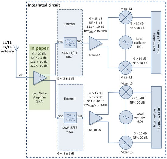
The proposed dual-band low-noise amplifier solution is different from other solutions in that it provides the amplification of two bands, L1 and L5, allowing the use of only one shared inductor for input impedance and noise matching. This saves a significant amount of area because, at frequencies associated with the L1 and L5 bands, the inductance of the inductor can be significant, e.g., from 8 to 20 nH, which involves an area of 300 µm × 300 µm or even up to 450 µm × 450 µm. Another advantage of using a single radio-frequency input for both amplified bands is the possibility of using a dual-band antenna—this involves further space savings and fewer external components.

The main drawback of the circuit is that it is non-trivial to achieve good impedance matching and noise matching at its input for both bands—as in a classic low-noise amplifier circuit. The circuit can be used in all types of multi-frequency radio transceiver systems and is probably one of the best solutions for such applications.

2. Design Considerations

The main task of the low-noise amplifier is to amplify the input signal. A high amplifier gain allows the total noise figure of the system to be reduced. Since it defines the lower limit of the total noise figure of the receiver circuit, it should provide the lowest possible noise figure. A low-noise amplifier should have good impedance matching at the input and output, good noise matching, sufficient gain linearity (IIP2, IIP3) and low current consumption.

The key parameters that characterize the LNA circuit are the voltage gain (G), noise figure (NF), input impedance matching (S11), output impedance matching (S22), isolation between output and input (S12), current consumption and the size of the device.

The most popular LNA architecture, i.e., a single-ended implementation with inductive source degeneration (Figure 2), is very appealing for low-power, low-cost designs due to the reduced number of passive elements (in comparison to the differential solution), low noise figure and small bias current. In Figure 2, one can see that a voltage follower is added to the output of the low-noise amplifier to achieve impedance matching of 50 ohms while maintaining high amplification.

The inductance Ls allows the real part of the input impedance to be controlled without adding noise. The Lgg coil determines a specific resonant frequency and is also responsible for noise matching. The Ld coil increases the gain of the amplifier and acts as a band-pass filter when combined with the capacitive load. The use of a cascode allows good isolation between the output and input to be achieved and minimizes the capacitive Miller effect. The capacitor Cin is used to cut off the DC component. Additionally, the Cex capacitor makes simultaneous impedance and noise matching easier while maintaining low power consumption.

Based on the solution presented above, we proposed a dual-band low-noise amplifier that saves the silicon area and allows the use of a single dual-band antenna.

3. Circuit Design

Figure 3 shows a new design of a dual-band low-noise amplifier based on the classical CS degenerated cascode LNA with a voltage follower. The main idea behind this solution is to use a single inductor Lgg at the radio-frequency input.

The Lgg coil is mainly responsible for noise matching and is responsible for establishing the appropriate resonant frequency at which the amplifier operates. Unfortunately, adjusting the amplifier with a single inductor on two bands is not trivial. Assuming that the center frequencies of the L1 and L5 bands are 1.575 GHz and 1.192 GHz, respectively, the average frequency of these two values is about 1.4 GHz. At this resonant frequency, the value of inductance Lgg will be pre-selected. It is necessary to assume the values of the currents polarizing the amplifying transistors M1 and M5—for example, 5 mA. The next key step is to properly select the size of the M1 and M5 transistors to obtain the best noise matching for each of the amplifier bands. The next step is to select the appropriate value of the Ls1 and Ls5 inductances to obtain a good impedance match. The Ls1 and Ls5 inductances are selected separately to obtain the best match for a given band (Ls1 = 0.82 nH, quality factor Q = 3.7 and Ls5 = 0.83 nH, quality factor Q = 2.98). In impedance matching, they play the main role in matching to the real part of the signal source impedance (matching to 50 Ω). By obtaining good results in terms of noise and impedance matching at the amplifier input, it is possible to check the effect of changing the Lgg inductance on the noise figure. With well-sized transistors and similar noise figures for both bands, changing the Lgg value will make it possible to obtain a better noise figure for one band while degrading the noise figure of the other band. If we have similar noise figures for each band and varying the Lgg value causes the described changes, this is the point at which the minimum obtainable noise figure at a given bias current has been achieved.

If we wish for the noise figure for both bands to be the same, its value will be higher than the analogous noise figure for a single-band low-noise amplifier. This research shows that a dual-band low-noise amplifier will have a higher noise figure for each band by about 0.4–0.6 dB. This is the cost of a two-band low-noise amplifier solution with one coil shared by both bands.

In the case of integrated LNA circuits, two different solutions for the use of inductors are commonly used. The first solution is to use externally mounted inductors on PCBs and the second is to use integrated inductors created in the process of manufacturing the integrated circuit. The main difference between these inductors is the quality factor.

The inductor mounted on the PCB is characterized by a Q factor that is over 10 times better than that of the integrated inductor. The high quality factor of the Lgg input inductor allows for much better noise matching (obtaining lower NF)—an inductor with a high inductance value has low resistance. In the case of using high-quality inductors in the drain Ld and source Ls of the amplifier, thanks to their lower resistance at the same inductance value, we are able to achieve a greater gain (there is no voltage drop in the inductor resistance). An inductor with a higher quality factor in the drain also affects the shape of the amplifier’s bandwidth—the amplifier becomes more narrowband. The main disadvantage of these inductors is that they require additional external components, which generates significant costs in mass production.

The main advantage of using integrated coils is that there is no need to use external components. With the right amplifier design, it is possible to obtain good noise parameters—meeting the specifications of a satellite navigation receiver with a significant margin. Integrated coils were used in the dual-band low-noise amplifier shown in Figure 3. The amplifier can operate in the dual-band mode as well as in single-band modes when only one band is amplified. In the single-band mode, only half of the amplifier is enabled, which allows for energy savings. The presented solution is optimized for the dual-band mode, which is the main mode of operation.

4. Results

Figure 3 shows the final version of the designed dual-band LNA circuit presented and analyzed in this paper. The following elements and their parasites were included in the dual-band LNA simulation: bonding pads with ESD protection diodes, bond-wire connections between the IC and package and decoupling capacitors. The RF input pad has been specifically designed to provide an adequate level of protection against ESD phenomena (HBM 2 kV) while minimizing the impact of the pad capacitance (Cparasitic = Cbondpad_plate + Cdiodes ≈ 1 pF) on the amplifier parameters. Taking all of these elements into account made it possible to obtain good agreement between the measurements and simulations. The section focusing on the simulation presents detailed results concerning the dual-band LNA.
Figure 4 shows the final layout of the designed dual-band LNA. The dimensions of the layout are 1389 µm × 749 µm. Lgg is the largest inductor and it is placed in the center of the layout. As can be seen, the largest part of the topography is occupied by five inductors, the pads occupy the second-largest area and the decoupling capacitors occupy the third. The active and passive elements that comprise the amplifier itself and the voltage follower occupy a very small area in comparison with the previously mentioned elements. In summary, using one coil less than in the case of two single-band amplifiers allows for significant savings in the silicon area.

4.1. Simulation Environment

The circuit was designed with the use of the Cadence software IC6.1.8-64b.500.21. The diagram was designed with the Schematic Editor L tool, the layout was designed with the Layout Suite XL tool and the simulations were performed with the ADE Explorer tool using the Spectre simulator. The parasitic elements were extracted with the Quantus parasitic extractor with a field solver for greater accuracy [13].
The voltage supply of the system was 1.5 V, and it was fed from a low-dropout regulator (LDO) or an ideal voltage source. The reference current for the designed block was 4 µA and was supplied from a temperature-stable, voltage-supply-stable and process-corner-stable current mirror. The dual-band LNA had a local current mirror to generate the required biasing voltages [13].
The circuits were simulated in the temperature range of −40 °C to 125 °C for various corner cases of the technological process with a voltage supply fluctuation of ±10% [13].

4.2. Simulation Results

Figure 5, Figure 6, Figure 7, Figure 8, Figure 9, Figure 10 and Figure 11 show the main characteristics of the dual-band low-noise amplifier (post-layout simulation in a typical process corner: 27 °C and nominal voltage supply 1.5 V). In all of the figures below, the grey shaded area defines the L1 and L5 band range, respectively.
The main parameters of the LNA at 1.575 GHz (L1 band center frequency) in the dual-band mode are voltage gain (GV) = 20.74 dB, S11 = −13.69 dB, S22 = −30.81 dB, S12 = −30.62, NF = 2.59 dB, current consumption (IDD) = 6.23 mA. The characteristics presenting the above amplifier parameters are shown in Figure 5 and Figure 9.
The parameters of the LNA at 1.192 GHz (L5 band center frequency) in the dual-band mode are voltage gain (GV) = 24.02 dB, S11 = −9.94 dB, S22 = −16.82 dB, S12 = −30.98 dB, NF = 2.47 dB, current consumption (IDD) = 6.23 mA. The characteristics presenting the above amplifier parameters are shown in Figure 6 and Figure 9.
The parameters of the LNA at 1.575 GHz (L1 band center frequency) in the single L1 band mode are: voltage gain (GV) = 21.28 dB, S11 = −12.56 dB, S22 = −26.16 dB, S12 = −31.11, NF = 2.46 dB, current consumption (IDD) = 2.91 mA. The characteristics presenting the above amplifier parameters are shown in Figure 7.
The parameters of the LNA at 1.192 GHz (L5 band center frequency) in the single L5 band mode are: voltage gain (GV) = 24.12 dB, S11 = −8.01 dB, S22 = −17.9 dB, S12 = −30.94 dB, NF = 2.46 dB, current consumption (IDD) = 3.55 mA. The characteristics presenting the above amplifier parameters are shown in Figure 8.
In Figure 5, Figure 6, Figure 7 and Figure 8, we can see how the input impedance of the LNA (S11 curve) changes during dual-/single-mode operation for both bands. The input matching characteristic of the S11 changes significantly between dual- and single-mode operation. In dual mode (Figure 5 and Figure 6), we have good impedance matching (“lows on the characteristic”) at both the L1 and L5 frequencies, whereas, in single-band operation, the matching for the disabled band is much worse (see Figure 7 and Figure 8).
The noise figure simulation in the dual-band mode is shown in Figure 9. The noise figure for the L1 band is NF = 2.59 dB and for the L5 band NF = 2.47 dB. In the case of single-band operation, the noise figure for the L1 band is NF = 2.46 dB and for the L5 band NF = 2.46 dB.
Figure 10 and Figure 11 show the characteristics of the one-decibel power compression. From the characteristics, we can see that the 1 dB compression point for the L1 band is P1dB = −37.72 dBm and for the L5 band P1dB = −34.72 dBm. This is a sufficient value for the GNSS input signal at the level of −125 dBm to −130 dBm.

To sum up the simulation results, the designed dual-band low-noise amplifier is characterized by good parameters in both the dual-band and single-band modes. Thanks to the ability to work in the single-band mode, the system gains the ability to save energy when needed.

4.3. Measurements

The designed low-noise amplifier may be powered by 1.5 V in two ways. The first way is to power the LNA from an external LDO located on the PCB. This provides an output voltage of 1.5 V, which is fed to the LNA’s VDD11_RFO power rail. The second option is to supply the LNA from an internal LDO (externally supplied with 1.8 V VDD18RF), giving an output voltage of 1.5 V to the LNA supply rail. Measurements show that the choice of power source for a dual-band low-noise amplifier has no effect on its performance. Simulations and measurements were performed using the internal LDO as the LNA power source.

  • Keithley 6512 electrometer—to measure the current consumption (up to 20 mA), used as an ammeter. The current consumption was measured using an external LDO with the ammeter connected in series (jumper J18, Figure 12).
  • Vector Network Analyzer Rode & Schwarz ZVL6—connected to the input (Figure 13 port P1 → RF_IN) and the output (Figure 13 port P2 → LNA_OUT1) of the low-noise amplifier for the L1 band. The circuit in which the S-matrix for L1 band was measured is shown in Figure 13.
To measure the L5 band, the measuring device was connected to the input (Figure 14 port P1 → RF_IN) and the output (Figure 14 port P2 → LNA_OUT5) of the low-noise amplifier. Before the measurement, the measuring instrument was calibrated, taking into account the cables connecting it with the measured system. The vector analyzer allowed the parameters of the scattering matrix to be determined. The circuit in which the S-matrix for L5 band was measured is shown in Figure 14.
  • EXA Signal Analyzer N9010A and external noise source (SNS)—the output of the noise source (Figure 15 port P1) was fed to the input of the low-noise amplifier (RF_IN); the output of the low-noise amplifier (LNA_OUT1) was connected to the input of the signal analyzer (Figure 15 port P1) for the L1 band.
For the L5 band, the measurement the output of the low-noise amplifier (LNA_OUT5) was connected to the input of the signal analyzer (Figure 16 port P1). Before the measurement, the measuring instrument was calibrated, taking into account the cables connecting it to the measured system. The signal analyzer allowed the noise figure (NF) of the tested system and the voltage gain of the signal to be determined.
Table 1 below summarizes the measurement and simulation results for the L1 band. The voltage gain characteristics (Figure 17) are almost the same and the difference in gain at 1.575 GHz is about 0.5 dB. This difference is due to the changes in the input matching characteristics (S11) and output matching characteristics (S22). Analyzing the measured characteristic of the input impedance matching (Figure 19), it can be concluded that the capacitance/inductance at the amplifier input is, in reality, slightly smaller than modeled in the simulations. This discrepancy may result, for example, from an inaccurate model of the wire connections to the QFN package—the model assumes an overly high value for bonding inductance. A small difference can be observed in the output impedance matching characteristics (Figure 20). In this case, we observe the opposite situation, i.e., the simulated inductance/capacitance in the output resonant circuit is smaller. This may be due to the bonding model, but also to the influence of dummy metal fills. The difference between the simulation and measurement in the S-matrix parameters is acceptable—the amplifier meets the assumed requirements. In order to correct the parameters, we can try to model the bonding better (since we suspect that the discrepancies result from it) or slightly modify the matching circuits at the input and output to take into account the differences observed between the measurements and simulations.
Table 2 below summarizes the measurement and simulation results for the L5 band. Comparing the voltage gain characteristics (Figure 22), we can see a significant difference in the center frequency of the amplified band (around 200 MHz), which is probably due to two aspects. The measured input impedance matching characteristic (Figure 24) is slightly shifted towards higher frequencies; additionally, in the L5 band, the input matching is worse by a few dB, which affects the voltage gain of the signal. The second aspect that we can observe in the S21 characteristic (Figure 26) is that the gain of the amplifier itself is lower by about 3 dB and also shifted towards higher frequencies. The impedance matching at the input can be influenced by bonding. When investigating the cause of the difference between the measurement and the simulation results regarding the voltage gain, the influence of the technological process’ dispersion on the voltage gain characteristics was verified by means of simulations. The impedance matching characteristics at the output matched perfectly (Figure 25). Despite the significant discrepancy in the voltage gain, the circuit has acceptable parameters.
Figure 27 presents a comparison of the noise figure simulation and measurement for the L1 band. The difference between the measured and simulated noise figure is 0.64 dB, which is acceptable. As can be seen in Figure 27, both characteristics have a similar shape, with a shift in the y-axis.
Figure 28 presents a comparison of the noise figure simulation and measurement for the L5 band. The difference between the measured and simulated noise figure is 1.06 dB, which is acceptable. As can be seen in Figure 28, both characteristics have a similar shape, with a constant shift in the y-axis.
The tables below (Table 3 and Table 4) compare the measurement and simulation results of the dual-band amplifier operating in the single-band mode. The results are very close to the parameters obtained in the dual-band mode.
The parameters of the dual-band LNA are summarized and compared with other published CMOS dual-band LNAs [4,7,10,14] in Table 5.
It can be seen that the proposed LNA achieved the highest voltage gain among the measured devices and had the best impedance input and output matching compared to other measured results. Comparing the noise figure with other measured circuits, it is better than circuit [7] but worse than circuit [10] by 0.56 dB. The worse noise figure than in circuit [10] may be due to many aspects and partly to the compromise between impedance and noise matching. In order to obtain better noise matching, we must sacrifice good impedance matching. In our LNA, at 1.57 GHz, we have input impedance matching at the level of S11 = −23.89 dB, while, in circuit [10], at 1.7 GHz, the input impedance matching is only S11 = −6.44 dB.
The simulation results are unfortunately difficult to compare directly because the results from [4,14] are based on circuit simulations and do not include parasitic elements resulting from the design of the circuit topography. For example, without taking into account the parasitic elements after topography extraction and the connections to the package, in the designed dual-band LNA, it is possible to obtain the noise level of NF = 1.8 dB for both bands, which is not realistic.
In addition, the amplifier from [4] has an off-chip input matching circuit—this allows much better noise parameters to be achieved at the expense of additional external components.
The figure of merit has been defined as follows:

F o M = G 1 d B + G 2 d B N F 1 d B + N F 2 d B 2 P D C [ m W ]

The dual-band low-noise amplifier’s microphotography is shown in Figure 29. The layout dimensions were 1389 µm × 749 µm.

5. Conclusions

The proposed dual-band low-noise amplifier is characterized by a high gain for both the L1 and L5 bands and a noise factor sufficient for navigation applications. One of its advantages is that it is well matched to 50 ohms at the input and output, which allows it to be easily integrated with other systems operating with an impedance of 50 ohms, e.g., antennas and filters. Another advantage is the possibility of turning off one band, e.g., when it is not needed, in order to save energy. This is very important for devices operating on batteries.

The measured parameters of the LNA at 1.575 GHz (L1 band center frequency) in the dual-band mode were voltage gain (GV) = 21.22 dB, S11 = −23.89 dB, S22 = −12.65 dB, S12 = −32.53, NF = 3.23 dB, current consumption (IDD) = 6.13 mA.

The measured parameters of the LNA at 1.192 GHz (L5 band center frequency) in the dual-band mode were voltage gain (GV) = 18.2 dB, S11 = −8.42 dB, S22 = −15.8 dB, S12 = −28.29 dB, NF = 3.53 dB, current consumption (IDD) = 6.13 mA.

The measured parameters of the LNA at 1.575 GHz (L1 band center frequency) in the single L1 band mode were voltage gain (GV) = 20.41 dB, S11 = −23.57 dB, S22 = −12.8 dB, S12 = −32.57, NF = 3.44 dB, current consumption (IDD) = 2.85 mA.

The measured parameters of the LNA at 1.192 GHz (L5 band center frequency) in the single L5 band mode were voltage gain (GV) = 18.16 dB, S11 = −6.9 dB, S22 = −16.3 dB, S12 = −27.79 dB, NF = 3.27 dB, current consumption (IDD) = 3.48 mA.

The designed system meets the specifications.


Source link

Daniel Pietron www.mdpi.com