1. Introduction
Infrared windows play an important role in infrared propagation, protecting internal detection signals, imaging systems, and dissipating heat generated by internal components during service. They are widely used in many fields such as space communication, remote sensing detection, and optoelectronic countermeasures [
1,
2,
3,
4,
5]. With the constant development of infrared technology, the working band of various infrared systems has gradually expanded from near-infrared and mid-infrared to far-infrared bands. The 3–5 μm and 8–14 μm bands are known as the “atmospheric window zone” due to their good transmittance to the atmosphere and minimal attenuation of radiation intensity. Therefore, the optical materials serving in the range of 3–5 μm mid-infrared and 8–14 μm far-infrared wavelengths have become important optical window materials. Commonly used infrared window materials include crystal materials such as Ge, zinc sulfide, zinc selenide, sapphire, as well as glass materials such as barium gallo-germanate (BGG) glass, gallium oxyfluoride (FGa) glass, and Zr-Ba-La-Al-Na (ZBLAN) glass. Among many infrared materials, ZnS material has an ultra-wide infrared transmission range, which can be transparent in an extremely wide energy range, with a very large transmission from visible wavelengths to just over 12 μm [
6,
7]. It monopolizes the mid to far infrared region that other optical glasses cannot pass through. Sulfur-based glass has a series of excellent optical properties such as extremely high nonlinear refractive index, adjustable composition, and low phonon energy [
6]. It can be directly processed into infrared optical lenses through precision molding, its preparation and processing costs are much lower than single crystal germanium, and its size is not limited. So, it is considered as the core material of the new generation of infrared optical windows [
8].
Then, in the aerospace environment with information technology rapidly developing, various infrared imaging systems also face serious electromagnetic interference (EMI), but these optical windows cannot be directly coated with opaque electromagnetic shielding materials, and it has become the weakest part in electromagnetic protection. Therefore, there is an urgent need for optical windows with high transparency, anti-electromagnetic shielding reinforcement.
Numerous types of transparent EMI shielding films exhibiting excellent shielding performance have been reported [
9,
10,
11,
12,
13,
14,
15,
16,
17,
18]. Among the novel EMI shielding materials, a continuous transparent conductive film, indium tin oxide (ITO), has played a significant role in transmitting visible light and shielding long wave EMI. However, due to the proximity of the passband, low transmittance of the substrate material, and limitations of continuous film materials, in terms of transmitting infrared light and shielding long wave EMI [
19,
20,
21], the metal mesh is still the only choice at present.
Excellent conductivity and good electromagnetic shielding capability are provided by metal mesh. Metal mesh films have special benefits in electrical conductivity, especially those composed of copper, silver, and gold [
22,
23,
24,
25]. Specifically, the random transparent metal mesh provides high optical transmittance and effective electromagnetic shielding, while also mitigating or even eliminating the starlight effect in the optical window [
26,
27,
28,
29,
30]. Clearer and more precise observed images are the outcome of this development, which also improves the optical system’s imaging capability. It follows that there have been numerous research results on metal mesh shielding films for optical windows in the visible light band, but there is relatively little research on optical windows in the infrared band. To date, metal mesh films have predominantly been fabricated using micro-nanofabrication technique which are costly and involve complex processes, such as laser direct writing [
31], ion beam etching [
32], ultraviolet lithography [
12], electric field-driven microscale 3D printing [
33], and nanoimprint lithography [
34]. In this study, we developed an IR transparent gold (Au) mesh optical window on a ZnS substrate. The irregular structure metal meshes were fabricated by the crack template methods based on a completely new perspective focusing on the period and line width ratio, which provided efficient and stable EMI shielding properties over a broad frequency spectrum and maintained high optical transparency in the infrared range. These findings serve as a theoretical foundation and technical reference for the engineering implementation of infrared transparent electromagnetic shielding optical windows.
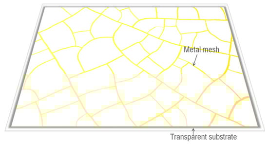
2. Structure Design and Simulation
Figure 1 shows the structure of the IR transparent EMI shielding window. Considering the balance between optical transmission and electromagnetic shielding performance. In theory, metal mesh transmittance is determined by its coverage ratio, incorporating both the average wire width and mesh spacing. The optical transmission (T) of different metallic meshes can be calculated using Equation (1) where a represents the average line width and g represents the average periodic length [
35]. This extended model also considers multi-layer mesh structures, with the number of layers represented by n. where Ts is the transmittance of the substrate.
The transmittance of ZnS glass itself is approximately 75% (in the wavelength 2–10 μm) [
36]. The transmittance variation curves of the substrate with single-sided metal mesh and double-sided metal mesh are calculated using Equation (1) for different ratios of aperture to line width, as shown in
Figure 2.
In metal mesh films, EMI shielding primarily results from electromagnetic wave reflection. Therefore, the shielding effectiveness depends on the metal mesh film’s electrical conductivity and can be further described as follows [
37]:
where is the wave impedance of free space and is the sheet resistance. Low sheet resistance materials generally provide enhanced EMI shielding, rendering low-resistance metal mesh films highly efficient for shielding applications.
Sheet resistance is determined by conductivity σ and skin depth δ, remaining independent of thickness (t), width (w), and mesh spacing (g). It can be evaluated by an Equation (3) [
38].
where σ is the conductivity (S/m), δ is the skin depth (μm), and t is the thickness of metal mesh film (μm).
Skin depth (δ) is related with the frequency (f) of incident plane wave and conductivity (σ) of metal mesh film, and it can be calculated by a function Equation (4).
where µ is the permeability (H/m), µ = 4π × 10−7 H·m−1, σ = 4.17 × 10⁷ S/m, and the EMI frequency band is from 1 to 18 GHz. According to the simulation calculation of Equations (2)–(4), the electromagnetic shielding effectiveness of the metal mesh with a certain aperture and line width (g/w) can be theoretically estimated.
3. Materials and Methods
3.1. Metal Mesh Preparation
After optical polishing, zinc sulfide with a thickness of 5 mm was chosen as the clear substrate for creating the Au meshes coated with EMI shielding infrared windows. Acetone, isopropanol, and deionized water were used to ultrasonically clean the substrates for two minutes each. The fractured templates were derived from a colloidal dispersion of acrylic resin. The acrylic resin colloidal dispersion was synthesized in-house (see
Supplementary Information). Drops of the colloidal dispersion based on acrylic resin were spin coated onto the substrate for 60 s and then dried at room temperature (25 °C) with 50% humidity to form crack template. A 300 nm-thick conductive Au film was deposited onto the cracked template via an e-beam evaporator (ZZS110, Chengdu Xingnanyi Vacuum Equipment Co., Ltd, Chengdu, China) at room temperature under a base vacuum of 5.4 × 10
−4 Pa, anode voltage of 200 V, and anode current of 1.5 A. The cracked template was removed via lift-off by immersing and sonicating the sample in 2-Acetoxy-1-methoxypropane (PGMEA) for 3–5 min [
39]. Finally, a conductive Au mesh were produced. The gold mesh preparation process is depicted in
Figure 3.
3.2. Microscopic Study
With the aid of an optical microscope (BX53M, Olympus Corporation, Tokyo, Japan), the morphologies of the Au meshes and fractured templates were investigated. After a 12-h drying phase, the film thicknesses were assessed using a probe profilometer (Dektak XT, Bruker, Bill Rika, MA, USA). The surface geometry of the cracked templates was measured using an Olympus OLS4100 laser confocal microscope. Custom image processing software was used to process these micrographs in order to analyze the width and size of each fracture zone.
3.3. Optoelectric Study
A FT&IR spectrometer (VERTEX70, Bruker, Bill Rika, MA, USA) was used to measure the spectrum dependencies of the optical transmittance of the Au meshes in the 2–15 μm. A four-probe head was used to measure the sheet resistance (ST2258C, Suzhou Jingge Electronic Co., Ltd., Suzhou, China).
3.4. EMI Shielding Measurements
Waveguide-to-coaxial adapters and a Vector Network Analyzer (E5080B, Keysight Technologies, Santa Clara, CA, USA) were used to assess EMI shielding effectiveness (SE) in the frequency range of 1–18 GHz in order to determine the scattering parameter (S21).