1. Introduction
The millimeter-wave (mmW) frequency band provides abundant spectrum resources for wireless communication, radar, and other applications, making high-speed communication and high-precision sensing possible, but the use distance of mmW applications is limited by atmospheric attenuation. On the other hand, the optimum maximum output power of a single transmitter based on current mature semiconductor technology at mmW frequencies due to the cutoff frequency (
fT) and maximum oscillation frequency (
fmax) of transistors, is far from meeting the demand. In order to extend the application scenarios of mmW, an mmW-phased array system becomes a promising solution. In phased-array systems, the front end of the transceiver occupies most of the area, which not only increases the cost, but even causes the phenomenon of side flap of the array antenna. Therefore, bidirectional transceivers that multiplex the transmit and receive links to significantly reduce the chip area have become a hot research topic in recent years [
1,
2,
3,
4]. Usually, bidirectional transceivers include modules such as a common transceiver antenna, a bidirectional amplifier, a bidirectional phase-shifter, and a bidirectional mixer. The bidirectional phase-shifters can be used to provide various phase differences between antennas in the array. In addition, when the operation frequency becomes higher, the antenna size shrinks to millimeter level, which is comparable with the chip. To further reduce the system area and improve the array density, the on-chip antenna (OCA) is employed in this system, making a fully integrated bidirectional transceiver become a reality. With the proper phase configuration, the system can transmit or receive signals with right-hand circular polarization (RHCP) or left-hand circular polarization (LHCP), which enables a high-output power reconfigurable phased-array for various applications.
With the continuous advancement of semiconductor technology, there is an increasing trend to replace traditional board-level systems with system-on-chip (SoC) solutions to enhance system integration [
5,
6,
7,
8]. SoC, as the name implies, integrates various circuits and the OCA directly onto the same silicon substrate, eliminating the need for lossy interconnections and maximizing integration efficiency. In recent years, most OCAs have been developed using silicon-based technologies such as CMOS and SiGe [
9,
10,
11,
12], while only a limited number of studies have explored the use of compound semiconductors [
13]. However, achieving high-performance OCAs on silicon substrates presents significant challenges. Notably, silicon substrates are characterized by a high dielectric constant and resistivity, both of which contribute to reduced radiation efficiency in OCAs [
8,
14]. Despite these challenges, the mmW frequency range presents an opportunity to realize OCAs with reduced antenna sizes down to the millimeter scale, making the integration of OCAs with silicon substrates feasible and promising for various applications. To address the aforementioned issues, numerous techniques have been proposed in the literature to enhance the radiation efficiency of the OCAs. In ref. [
15], a large silicon lens is placed on the back of the chip substrate to reduce surface wave and substrate mode effects. By employing a silicon lens, the antenna achieves a 31% antenna efficiency and 18.9 dBi directivity at 220 GHz. As a result, this yields an antenna gain of 13.8 dBi. This method necessitates a high cost and a large form-factor silicon lens, making it unsuitable for low-cost or highly integrated applications. In ref. [
12], localized back-side etching (LBE) technology is employed to implement a highly efficient
D-band OCA using the SiGe process. This costly method alters the standard silicon substrate, limiting its practicality in widespread applications. In ref. [
16], the resistivity of the silicon substrate is increased through proton implantation. Although this method enhances the radiation efficiency of the antenna, it may also reduce circuit performance and induce a latch-up effect. The processing technology is complex, making it unsuitable for low-cost applications. In ref. [
9], substrate thinning is applied to mitigate surface wave and substrate mode effects. This method requires processes, increasing both the cost and the risk to silicon substrate stability. In ref. [
17], an artificial magnetic conductor (AMC) reflective surface is constructed in the M1 layer of the silicon substrate; the AMC serves to isolate the electromagnetic wave, thereby reducing substrate losses. This method requires constant optimization of the AMC structure and necessitates a wideband technique due to the short distance between the top metal and M1 layers, rendering the OCA design more complex. In conclusion, the current techniques enhance OCA performance by modifying the substrate of the standard process. These post-processing costs, and non-standard processes are less compatible with large-scale circuits. Therefore, a method utilizing standard CMOS substrate for high-performance OCA design is desirable.
Traditionally, the purpose of IC packaging was to ensure mechanical and thermal stability, primarily protecting the chip from physical damage without offering electrical properties. This paper proposes transforming the use of PCBs as chip packages into functional housings to enhance the radiation efficiency of the OCA by decreasing electromagnetic wave reflection at the silicon substrate–air interface, achieved through low-loss PCBs that offer wave-impedance matching. Furthermore, integrating the OCA with RFIC reduces high-frequency interconnection loss. The antenna structure is designed as a
D-band bowtie OCA using a standard TSMC 40 nm CMOS process without any post-processing [
18,
19], and hollow bowtie design facilitates a wide frequency band and excellent matching characteristics. Notably, the radiation performance of the antenna is enhanced solely by using the PCB package [
20,
21]. This design achieves efficient integration, as evidenced by its compact footprint on a single chip, while ensuring reliable radiation performance. Circular polarization is achieved by arranging two pairs of antennas orthogonally, without a significant increase in the chip area.
2. Theory and Geometry of the Designed On-Chip Antenna
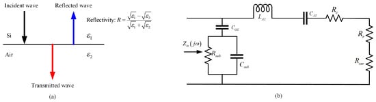
In designing OCAs on silicon substrates, a primary challenge is the downward radiation caused by the high dielectric constant of the silicon substrate, which, combined with low resistivity, results in significant absorption of radiation energy within the substrate. As illustrated in
Figure 1a, from an optical perspective, the rays emitted by the antenna and incident upon the interface between different media are refracted according to Fresnel’s laws. For a silicon substrate with a high dielectric constant (
εr = 11.9) and air with a low dielectric constant (
εr = 1), approximately 70% of the electromagnetic wave is reflected. This phenomenon is analogous to a severe impedance mismatch in a circuit. To enhance understanding and design of the OCA, an equivalent circuit model is employed to simulate its electromagnetic characteristics and to analyze the relationship between antenna efficiency and substrate characteristics. Equivalent circuit models simplify the antenna’s radiation and loss effects into a combination of fundamental components, such as resistance, inductance, and capacitance, thereby making the analysis of antenna performance more intuitive. The equivalent circuit model typically includes parameters such as radiation resistance, surface wave impedance, and parasitic capacitance, which directly influence the radiation efficiency and impedance-matching of the antenna.
As illustrated in
Figure 1b,
Cox represents the equivalent capacitance formed by the SiO
2 layer;
Rsub and
Csub represent the equivalent resistance and capacitance of the silicon substrate, respectively;
LAT and
CAT represent the equivalent inductance and capacitance of the antenna itself, respectively; and
Rr,
Rsur, and
Rc represent the antenna’s radiation resistance, surface-wave resistance, and conductor loss resistance, respectively. In this manner, the input impedance of the OCA can be expressed as
which
and
Therefore, the radiation efficiency of the antenna can be expressed as
Here,
Re[
Zin (
jωAT)] represents the real part of the antenna’s input impedance, and
ωAT represents the antenna’s resonant angular frequency.
Noting that
Rsub and
Csub are related to the resistivity
ρ and the dielectric constant
εr of the silicon substrate (
,
), and combining the aforementioned equations, we obtain
It can be concluded from the above that, at constant radiation resistance, both decreasing the resistivity and increasing the dielectric constant of the substrate result in an increase in Re[Zin (jωAT)]. This leads to reduced antenna efficiency, explaining the low efficiency of OCAs fabricated on silicon substrates.
To address the above issue and enhance antenna efficiency, extending the electromagnetic field into a low-loss dielectric minimizes power loss within the substrate. This concept is akin to early researchers who introduced superstrate layers on printed antennas to enhance radiation performance [
22]. It has been demonstrated that when the parameters of the superstrate layers are correctly selected, resonance conditions will be generated, significantly improving the gain and radiation of the antenna. The thickness of the superstrate layer plays an important role in achieving resonance conditions. The superstrate layers act as impedance converters, enhancing the coupling between the antenna and free space. In terms of transmission line equivalence, when the thickness is
nλd/4 (where
n = 1, 3, 5…), the antenna will exhibit better radiation. However, it has been observed that when
n > 1, the superstrate layer becomes too thick, leading to the degradation of surface wave excitation and the accompanying radiation pattern. Optimizing both the substrate and superstrate layer thickness is crucial for achieving optimal antenna performance. Research has shown that the best performance occurs when the superstrate layer thickness is
λd/4, where
λd represents the wavelength in the dielectric.
The packaging of integrated circuits is a critical finalization step before practical deployment, serving to protect the circuits from environmental and physical challenges. This protective role is especially significant when an OCA is integrated into the chip. In such cases, the packaging must not only protect the physical integrity of the chip but also preserve the operational characteristics of the antenna. For OCAs, the dielectric constant and loss tangent of the packaging material are crucial for the antenna’s performance. The presence of the package modifies the effective dielectric constant around the OCA, thereby altering its operating frequency and input impedance. This necessitates a comprehensive simulation that integrates the antenna with its intended packaging to evaluate the antenna’s operational state in real-world conditions. While the inclusion of an OCA introduces complexity to the chip packaging process, it also offers the opportunity to customize the packaging to optimize antenna performance. By carefully designing the package, it is possible to facilitate the effective radiation of backside emissions into free space, thereby improving the antenna’s efficiency and functionality. This paper mitigates the challenge of electromagnetic wave reflection at interfaces with high dielectric constant ratios by introducing a PCB layer between the silicon substrate and air, thereby enhancing the radiation performance of OCAs. Specifically, the inclusion of a PCB layer serves as an intermediary that reduces the mismatch in dielectric properties between the high dielectric-constant silicon and the surrounding air, which is essential for minimizing energy loss due to reflection.
To validate this concept, a D-band bowtie antenna was designed using the 40 nm CMOS process, incorporating a PCB package directly into the design framework. The PCB acts as a guiding dielectric, effectively absorbing the excited electromagnetic waves, with the primary radiation consequently being emitted from the back of the PCB. It is worth noting that even though the gain enhancement in this design is not as high as loading a conventional silicon lens, this design does not require complex post-processing steps, streamlining the manufacturing process while ensuring effective performance. Additionally, in the CMOS process, a critical requirement for integrated circuit design is maintaining appropriate metal density, which necessitates design rule checks (DRC). The metal surface area of the antenna can impose significant design constraints due to these metal density requirements. Consequently, achieving the desired radiation performance with minimal metal usage becomes essential. The analysis of the current density on the surface of the bowtie antenna indicates that the majority of the surface current concentrates along the edges, with significantly lower current density in the central regions. Based on this observation, it was concluded that removing most of the metal in the center would not significantly impact the antenna’s gain, bandwidth, or center frequency. This insight informed the design of the hollow bowtie antenna, which meets the strict metal density requirements while preserving the desired radiation performance.
Figure 2 illustrates the configuration of the designed bowtie OCA. The OCA is connected with two bidirectional transceivers, which consists of a bidirectional amplifier, a bidirectional phase shifter, and a bidirectional mixer, so the system can both receive or transmit RHCP/LHCP signal through setting their phase shift. The OCA assembly includes both a chip and a PCB package. To ensure proper chip functionality, external bias voltages and inputs must be supplied. Consequently, bonding wires are required to connect the chip pads to the printed circuit board (PCB) for transmitting electronic signals, and these bonding wires should be placed away from the antenna to minimize interference with antenna performance. As the designed OCA radiates minimal energy upwards and primarily directs radiation downwards, the impact on performance is negligible. We examine the impact of bonding wires on antenna gain, specifically within a 0.1 dBi range. The package primarily consists of two PCB layers. The chip is bonded to the underlying PCB with an adhesive. The adhesive employs a thin epoxy resin, with an optimal thickness of no more than 10 µm, to secure the chip to the carrier and minimize performance degradation [
23]. The top layer can be fabricated from cost-effective FR4, which offers structural integrity and environmental protection, while the bottom layer necessitates the use of low-loss Rogers3003 to enhance radiation performance.
The chip is fabricated using the 40 nm CMOS process and includes a silicon substrate topped with an oxide layer. It features 10 metal layers within the oxide layer, with the topmost layer utilized for antenna design due to its optimal conductivity and minimal loss characteristics, measuring 3.5 µm in thickness. The structure includes two pairs of symmetrical bowtie antenna to facilitate circular polarization and incorporates a central opening to reduce electromagnetic coupling with the feedline. Adjustments to the antenna’s resonant frequency are achieved by modifying the lengths LA of the antenna arms, while the input impedance is tuned by adjusting the width Wf of the feedline.