1. Introduction
Surface-enhanced Raman scattering (SERS) has become an indispensable tool for chemical and biological detection [
1,
2,
3], forensic analysis [
4,
5], molecular bioimaging [
6,
7], and environmental monitoring [
8,
9]. This is due to the inherent characteristics of Raman scattering, which include high sensitivity, high resolution, and specificity to molecular structures [
10,
11]. These attributes provide rapid, accurate, and detailed fingerprint information for molecular recognition and detection. Currently, the mechanisms of the SERS enhancement are explored from two perspectives: the chemical enhancement mechanism and the physical enhancement mechanism. The former primarily refers to the change in polarizability when a molecule interacts with a metal surface, providing enhancement factors of 10–1000 [
12,
13]. It can have contributions from three processes. First, when a molecule adsorbs on a metal surface, the redistribution of the electron cloud of the molecule changes its polarizability. Second, when a molecule has a strong chemical interaction with the metal surface, a surface complex can form, which changes the polarizability of the molecule. Third, when the excitation wavelength matches the energy difference between the highest occupied molecular orbital or lowest unoccupied molecular orbital of the molecule and the Fermi level or a surface state of the metal substrate, charge transfer between the two may occur. This photon-driven charge transfer can increase the polarizability of the molecule [
14,
15]. Compared to the chemical mechanism, the physical enhancement mechanism can provide enhancement factors of up to 10
15, enabling the development of a single-molecule SERS monitoring platform [
16,
17,
18]. Physical enhancement arises from a significant increase in the local electromagnetic field near metallic surfaces due to the excitation of localized surface plasmon resonance (LSPR) [
19]. LSPR manifests as optical resonance, with its frequency being highly dependent on the size and shape of the particles, inter-particle distance, and the surrounding medium [
20,
21,
22,
23]. In this sense, by adjusting these parameters, the resonance wavelength can be finely tuned from the visible to the near-infrared range to match the spectrum of the analyte molecules. LSPR has been extensively applied in sensors, optical device fabrication, and surface-enhanced spectroscopy, with efficient SERS being one of the critical research directions.
Noble metals, such as gold and silver, are more frequently chosen as SERS substrates due to their low loss and high scattering enhancement capabilities [
24,
25]. However, it is noteworthy that they have limitations in terms of stability and biocompatibility [
26]. Few SERS substrates can function effectively in highly alkaline or acidic environments, posing a significant challenge in certain applications. For example, many aerosol droplets present strong acidity or alkalinity. Droplets of a phosphate buffer solution with a size of about 20 μm, prepared from a bulk solution with a neutral pH, actually display strong alkalinity [
27]. Additionally, when the particle size is smaller than 2.5 μm, droplets produced from (NH
4)
2SO
4–H
2SO
4 solutions are more acidic than the bulk solution, which already exhibits extremely strong acidity [
28]. Therefore, there is an increasing need to develop SERS substrates capable of functioning under extreme pH conditions. Molybdenum (Mo) is a crucial high-melting-point, high-tolerance transition metal known for its exceptional intrinsic optical properties and chemical stability. Mo-based micro-nano structures have demonstrated exceptional absorbing and tunable performance, from visible to near-infrared wavelengths [
29,
30,
31]. Additionally, Mo is commonly adopted into alloy materials to enhance overall corrosion resistance [
32,
33].
This study proposes a highly tolerant Mo-based truncated cone array structure as a SERS substrate. Each individual truncated cone unit cell has a height of 1.8 μm, with top and bottom surface diameters of 3.7 μm and 5.6 μm, respectively. The array has a tunable period ranging from 8 to 12 μm. The plasmonic resonance and local field characteristics of the unit cell structures are comprehensively analyzed using the finite-difference time-domain method. Additionally, variations in the SERS signal from the molecular probe Rhodamine 6G indicated the presence of tunable localized surface plasmon resonance properties, achievable through regularly patterned structure arrays designed via ultraviolet lithography. This research approach can be applied not only to Mo-based structures but also to other metallic materials.
2. Materials and Methods
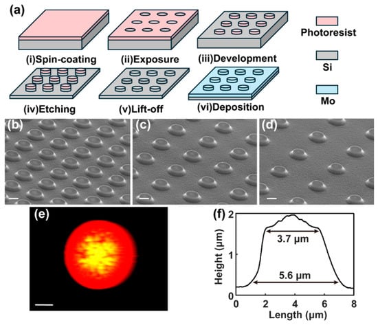
Figure 1a presents a schematic diagram of the entire Mo-based ordered structure array preparation process. The arrays of truncated cones were fabricated using the combination of ultraviolet lithography, inductively coupled plasma etching, and magnetron sputtering. Prior to processing, the native oxide layer of the silicon (Si) substrate was stripped in a 2% hydrofluoric acid solution, followed by ultrasonic rinsing for 15 min successively in acetone, absolute ethanol, and deionized water. After drying with nitrogen gas flow, the Si substrate was spin-coated with a layer of photoresist (RZJ-390PG, Ruihong Electronic Chemical Co., Ltd., Suzhou, China) at 4000 rpm for 40 s, followed by a 10 min vacuum bake at 120 °C. Periodic arrays of dots were patterned into the photoresist layer using an ultraviolet lithography system (TTT-07-UV litho, TuoTuo Technology, Suzhou, China). The dot diameters were designed to be 4 µm, with gaps ranging from 4 to 8 µm, and were arranged of 100 × 100 dot arrays. The exposure time was set to 120 ms with an exposure intensity of 1370 mW/cm
2. Following patterning, the resist was developed for 60 s to create the photoresist round patterns. The inductively coupled plasma etching process was carried out in 50 sccm of CHF
4 in a chamber held at a pressure of 100 mTorr, with a radio-frequency power of 300 W. The gas flow rate, gas pressure, and radio-frequency power show an inverse correlation with the height of the truncated cones, where an increase in these parameters leads to a gradual reduction in height. In contrast, these parameters have a direct positive correlation with the verticality of the sidewalls, making them more vertical as the parameters increase. Once the pillars were formed, a lift-off process with acetone was performed to create a Si mask for the subsequent magnetron sputtering. A 500-nm layer of Mo was sputtered onto the surface of the Si truncated cones using a magnetron sputter, forming the final arrays of Mo-on-Si micro-nano structures. The surface morphology of the fabricated Mo-based truncated cones was characterized using a scanning electron microscope (SEM, Supra 60, Zeiss, operated at 10 kV, Oberkochen, Germany).
Figure 1b–d show the different periods of the fabricated Mo truncated cone arrays, with a period range of 8 to 12 µm. As observed from the SEM images, the structure exhibits excellent uniformity and can be fabricated consistently and reproducibly. Additionally, an atomic force microscope (AFM) was used to extract the precise dimensions of individual unit cell structures, as shown in
Figure 1e,f. The results indicate that the truncated cones have a top surface diameter of 3.7 µm, a bottom surface diameter of 5.6 µm, and a height of 1.8 µm.
3. Results
Numerical simulations of the fabricated Mo-based truncated cone structures were carried out by the finite-difference time-domain method (Ansys Lumerical FDTD, Swanson Analysis Systems, Inc., South Pittsburg, PA, USA). The periodic boundary conditions were set for the x and y directions, whereas a perfectly matched layer boundary condition was selected for the z direction. In the model, the dimensions of the unit cells and the periodicity of the arrays were obtained from AFM image measurements. The incident laser source was modeled as a plane wave with a wavelength range of 300–800 nm. A tetrahedral mesh was employed, with a minimum mesh size of 20 nm. The refractive index of Mo is sourced from M. M. Kirillova [
34]. Localized electric field distributions on the truncated cone arrays with periods of 8 µm and 12 µm were simulated for the excitation wavelength of 532 nm, as shown in
Figure 2a,c. The white dotted lines indicate the outer contours of the Mo truncated cone structures. It is seen that the high electric field is symmetrically distributed on the two opposite sides of the truncated cone due to LSPR. This distribution is characteristic of dipolar resonance in plasmonic disc-shaped nanostructures [
35]. Due to the scattering from the truncated cones themselves, the localized electric field is further enhanced. Between the two adjacent cell structures, the electric fields become highly localized, forming a series of “hot spots”. Generally, the closer the proximity between two cells, the more pronounced the hot-spot effect and the greater the amplification of the Raman signals. Thus, the hot-spot-mediated enhanced electromagnetic field intensity is the primary reason for the high detection sensitivity of SERS [
36,
37]. It is noteworthy that the Mo-based truncated cone structures with an 8 µm period exhibit a stronger local field intensity of 6.23. However, when the period is increased to 12 µm, the field intensity decreases to 5.35.
Figure 2b,d show the normalized maximum electric field intensities of (a) and (c) in the Z-axis direction, respectively. This change in period causes the resonance peak to gradually shift away from 532 nm, resulting in a decrease in localized electric field intensity in this wavelength band. The tunability of LSPR is one of its important characteristics. Along the Z-axis, the incident light undergoes a phase shift, forming a longitudinal standing wave with nodes and antinodes located at the bottom metal layer and the open end of the Mo truncated cone, respectively. Along the X-axis, the closely spaced Mo-based truncated cone array creates a vertical gap plasmon resonator, functioning as a lateral Fabry–Perot resonator within a metal–insulator–metal (MIM) waveguide, where air acts as the insulating medium. This configuration exhibits enhanced electric field behavior [
38]. The efficiency of Raman scattering is influenced not only by the localized electric field enhancement but also by the size of the hot-spot area. A larger hot-spot area increases the probability of Raman molecules being effectively adsorbed in the plasmonic resonator. In this work, within the interstitial regions of the truncated cone structures with an 8 µm period, 67.36% of the area exhibits a field enhancement factor greater than 1, while 23.55% of the area has a field enhancement factor greater than 3.
Figure 2e depicts a dark-field optical microscope image of the truncated cone structures with a period of 8 µm. This ordered structure array exhibits good morphology, with a flat surface and no obvious defects.
Figure 2f shows the corresponding detected hot spots of
Figure 2e. Brighter spots are evident, indicating higher light scattering intensity in the response area compared to the surrounding regions. Therefore, the hot spots in the image typically correspond to locations where the localized field is enhanced, predominantly appearing between the two units cell structures, consistent with the calculations in
Figure 2a. The scattering spectrum result (
Figure 2g) further indicates that the localized field enhancement occurs over a spectral range of 500–800 nm, with a peak around 670 nm.
Figure 3a presents the SERS spectra of Si, Mo film, and the Mo truncated cone structure arrays with periods ranging from 8 to 12 µm. The SERS properties were firstly measured using a micro-Raman spectrometer (InVia Reflex, Renishaw, Wotton-under-Edge, UK) with an excitation laser wavelength of 532 nm. The laser was focused on the sample surface to a beam spot of approximately 2 µm using a 50× objective. The laser power at the sample surface was measured at 3 mW, and the acquisition time for each spectrum was 10 s. The concentration of Rhodamine 6G molecules was 1 × 10
−5 M. It can be observed that the characteristic Raman peaks of the Rhodamine 6G molecules were significantly enhanced for all truncated cone arrays compared to the planar Mo film. Specifically, the peak observed at 611 cm
−1 is attributed to the in-plane bending of the C-C-C ring in R6G. The peaks at 780 cm
−1 and 1190 cm
−1 correspond to the out-of-plane bending of C-H bonds, while the peaks at 1367 cm
−1, 1506 cm
−1, and 1650 cm
−1 are associated with aromatic stretching vibrations [
39]. As the array period increases from 8 µm to 12 µm, the intensity of all Raman peaks gradually decreases. Among the observed peaks, the one at 611 cm
−1 shows the most minor relative decrease, dropping from 4.4 × 10
4 to 3.3 × 10
4. After two repeated experiments, the average decrease rate was 27.62%, with a corresponding standard deviation of 0.0262. In contrast, the peak at 1650 cm
−1 exhibits the most significant relative decrease, declining from 3.3 × 10
4 to 1.92 × 10
4, with an average decrease rate of 40.24%, with a standard deviation of 0.0156. Overall, the average reduction in Raman intensity was 33.93%, with a standard deviation of 0.0631. The inserted SEM images show top views of the arrays with different periods, which have a scale of 10 µm. This decrease in SERS intensity is attributed to the reduction in localized field strength, as discussed in
Figure 2. It is noted that when using a Si substrate directly, these Raman peaks of Rhodamine 6G are completely indiscernible (see black line in
Figure 3a). This highlights the high efficiency of Mo micro-nano structures as SERS substrates.
On the other hand, the applicable wavelength range of this SERS enhancement is equally important for practical applications. The absorption spectrum of Rhodamine 6G at a concentration of 10
−5 M was measured at room temperature with a spectrophotometer (UV3600, Shimadzu, Kyoto, Japan) in the range from 400 to 700 nm, as shown in
Figure 3b. One can conclude that when the wavelength exceeds 550 nm, the absorption efficiency of the Rhodamine 6G solution decreases rapidly. Under the enhancement of the Mo micro-nano structure array, although the intensity of characteristic Raman peaks of the Rhodamine 6G molecules is significantly reduced, they can still be clearly distinguished.
To estimate the reproducibility of the SERS signals on the substrates, SERS mapping was conducted for each array.
Figure 4a shows the optical micrograph of the mapping area of the Mo truncated cone array with an 8 µm period, and
Figure 4a–c show the SERS intensity mapping of the 611 cm
−1 band, which exhibits the highest Raman scattering intensity, the 1367 cm
−1 band, which is near the average value, and the 1650 cm
−1 band, which has the lowest Raman scattering intensity, respectively. The mapping area is 40 µm × 40 µm. The intensity distribution patterns in the three maps are similar. The black circle indicates the boundaries of the structure. The intensity of mapping image (a) is relatively higher than that of mapping images (b) and (c). Generally, the SERS intensity is uniform across the analyzed area, indicating good reproducibility. Some dark spots were observed, which were attributed to surface contamination.
Figure 4d shows the optical micrograph of the mapping area of the Mo truncated cone array with an 8 µm period. The white rectangular area indicates the region where Raman scattering was measured. Each point in the scanned area was measured two times. The relative standard deviations for the three wavenumbers of 611 cm
−1, 1367 cm
−1, and 1650 cm
−1 were 0.1001, 0.1069, and 0.0759, respectively. For practical applications, the fabricated Mo-based truncated cone arrays can be used to fabricate sensitive and reliable SERS sensors for detecting solution concentrations. Solutions with concentrations ranging from 10
−3 to 10
−5 M were prepared and applied to the Mo truncated cones substrate with a period of 8 µm for SERS analysis.
Figure 4e illustrates the linear relationship between the spectral intensity at 1367 cm
−1, which is close to the average Raman scattering intensity, and the concentration of Rhodamine 6G. All data points represent the average values obtained from two replicate experiments. The concentration was quantified, and the intensity variation was represented by the empirical equation: Log I = 0.53 Log C + 15.7, with a correlation coefficient of 0.9819. These results indicate that the proposed Mo-based truncated cone arrays can be effectively used in the development of high-tolerance biochemical sensors.